Why and What?
In recent years, several non-volatile memory (NVM) technologies have demonstrated great potential in resolving the critical challenges of modern memory systems, namely density, latency, and power. Since these state-of-the-art NVMs offer high storage capacity and reasonable performance with low power consumption, extensive research is being carried out to fit these NVMs into the different layers of the existing memory hierarchy.
Even though existing studies have explored theoretical potential of the NVMs and offered unprecedented insight into memory management techniques for NVM systems, the publicly available data, for most part, is generated from overly simplified analytic models or from simulation based studies that have not yet been verified for real devices. Accurate characterization of real device samples is essential for understanding the true potential of the emerging non-volatile memories (NVMs), and identifying their optimal placement in the memory hierarchy. Though NVM products are now available from different manufacturers, lack of appropriate NVM controller and evaluation platform in the public domain is the main challenge in extracting empirical data from these emerging NVM technologies.
To address this challenge, under the supervision of Dr. Myoungsoo Jung, we have developed OpenNVM - an open sourced Field-Programmable Gate Array (FPGA) based NVM evaluation and characterization platform equipped with an efficient, highly configurable NVM controller. Our OpenNVM can cope with diversified memory transactions and cover a variety of evaluation workloads without any FPGA logic block updates. In our design, while evaluation scripts are managed by a host, all the NVM-related transactions are handled by our FPGA-based NVM controller connected to the hardware circuit board that can accommodate different types of NVM product and our custom-made power measurement board.
This open scheme has been developed to generate exhaustive, empirical data of emerging non-volatile memory in a configured, programmable FPGA based hardware prototype in order to serve the area in research on memories especially non-volatile type. This characterization platform can extract the critical parameters of the non-volatile memories, such as - * Latency * Power Consumption * Retention time * Non-Volatility * Endurance
Overview
Our OpenNVM platform is required to execute different categories of memory request and diverse workloads, while it needs to accommodate various types of NVM devices as well. However, once the logic gates are designed and implemented, it is challenging to update their logic blocks to cover a wide spectrum of such execution conditions. To address this, we separate the FPGA logic into three major different modules as shown in Figure 6 : i) communication module, ii) operation manager, and iii) memory controller.
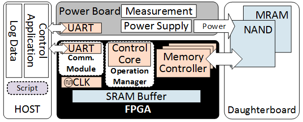
Specifically, the communication module is responsible for receiving the commands and reporting the results through the protocol we defined, and the operation manager composes specific NVM requests based on the commands requested by the host and forward it to the underlying memory controller. The memory controller then generates specific signals for different types of NVM devices. This logic design of ours allows us to not only cover diverse NVM memory products but also flexibly control a broad range of memory workloads, as the NVM operations and access patterns can be simply composed and requested from the host (without any FPGA modification). Lastly, we built a customized printed circuit board (PCB) that connects the FPGA and the real NVM device through a veryhigh-density cable interconnect (VHDCI) and can select power sources for measuring NVM device power consumption. In this PCB design, we also expose all test pins connected to external logic analyzer, and can connect different types of chip sockets.
Key Features:
- Support for evaluating a wide range of NVM products (MRAM, and NAND Flash at present)
- Broad spectrum of characterization parameters - access speed, non-volatility, standby and active power, and endurance.
- Synchronous, single, burst or chunk DUT access with adjustable read or write latency @ 500MHz clock speed.
- Able to Process 40 high speed I/O control to the DUT
- 2nS precision in timing measurement
- Flexible hardware prototype and re-configurable controller design in Verilog HDL
- Automatic latency detection and power measurement
- Supports two modes of operation:
- User interactive mode
- Speed-test Mode
This wiki is a full step by step tour, so that one can easily mimic this to build their own FPGA scheme, as a memory-controller either to characterize NVM or build any new NVM-system. This will also help in directing many FPGA based IC test and building any FPGA based prototype.
If you feel that OpenNVM was helpful for your research, we would sincerely appreciate if you cite our work published in ICCD'2015.