Daughter Board (PCB) Design
Why do we need a PCB?
Since our basic goal is to connect the NVM to the controller, theoretically, a simple breadboard could serve the purpose. However, it will make the connection and the debug process exponentially complex with increasing number of I/Os and density of the pins. For example, to connect the MR2A16A MRAM chip we need 320 I/Os. To deal with this, we used VHDCI and SATA connectors with our PCB which was almost impossible with regular breadboards.
PCB Design Process
The daughter board in our Open-NVM is a custom printed circuit board (PCB) designed to work as a pedestal for the NVM chip under test, and provide the required connectivity between the chip and the FPGA board. If you are using same development board (Nexys 3) like us to build the memory controller and its VHDCI expansion, and same NVM products (e.g., Everspin - MR2A16A (MRAM) or Micron - MT29F64G08EBAA (TLC NAND Flash)), you can directly use our design (gerber) files (http://open-fpga-nvm.github.io/source/) and components for PCB order and assembly. And when you do so, it is assumed that you have clear understanding about purpose and type of each I/O, PCB Layout, components etc.
The PCB design for the daughter board can basically be break down into the following steps:
- Download a PCB design tool
- Select required components
- Design and manufacture the PCB, and
- Assemble the daughter board
The whole design cycle may take from couple of days to couple of weeks depending on designer's level of expertise and the chosen PCB manufacturer's turnaround time plus shipping and handling delay etc.
1. PCB Design Tool
Some of the currently popular PCB layout tools are Allegro (Cadence), Pads (Mentor Graphics), Altium Designer, Eagle (Mac OS compatible) etc. Each of these tools have their unique advantages and limitations, and all of them are proprietary software. Instead we chose to use PCB Artist, a tool offered by the vendor 'Advance Circuits' we chose for manufacturing the PCB for us.
While selecting the PCB design tool one should look out for -
- Compatibility with required PCB layout-precision and latency
- Ease of LVS and DRC debug and fixing
- Availability of footprint wizard
- Efficient Auto-routing and Auto-placement
- Manageable libraries and files
- Kernel compatibility
- Smooth learning curve, and
- Budget (Price)
2. Selecting Required Components
Before actually designing the PCB, one needs to decide on the components, as that changes the design drawing. Some of the components are pretty specific, while others may be offered from various vendors with different footprint. Selection should have been done depending on * Price * Footprint * Electrical property * Minimum quantity to order and number of quantity you like to have
There are various reliable websites you can search and order your components, like Digikey, Amazon. Sometimes getting specific research components can be challenging, as they may not be in production or the distributor would only agree to supply in large amount. We would like to thank America II Electronics for helping us out with the TLC NAND Flash chips.
In our case, for each TLC-NandFlash PCB we required
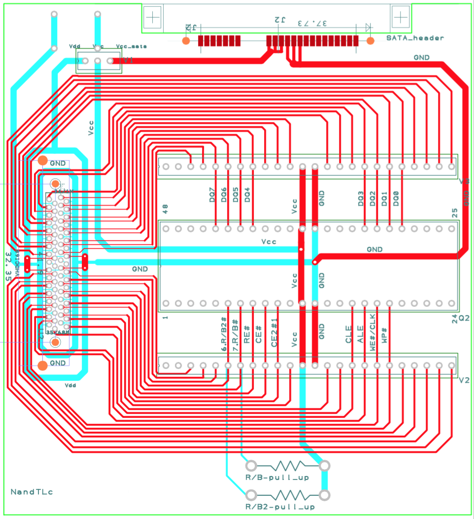
- One VHDCI-68 connector in order to connect our FPGA development board
- One SATA connector to connect our power measurement board
- Two 24-0.1"pitch DIP socket strips(breakable) to plug in 48 pin DIP sockets for TLC-Nand
- Pin headers (>50 counts) for alternate line option and debug/probing.
We also used VHDCI cable connector (male to male type, as both of our development board and PCB has male type VHDCI), and header-jumper for line selection.
3. Design and Manufacture the PCB
For an efficient PCB design and for avoiding trial and error repetition, one should develop your system and test it using breadboard, or build and test it with a layout schematic. All the renowned PCB tools offer schematic along with it but not testability. We have tested partly with breadboard and layout ours using PCB Artist. The steps we followed for designing our daughter board PCB are:
Create Component: For this, there are three basic steps: 1. Create schematic symbol: for using it in the PCB schematic, 2. Create PCB symbol: This is the physical footprint that your are laying out and will be used in the PCB, and 3. Create Component: for consistency between your schematic and layout.
There are thousands of components available and ready to use from millions/billions of components in the market. Instead of looking for available library to your tool, it may be better to build our own ones, as this takes much less time - once you are familiar with the tools and PCB-basic. However, for the more complex components, such as VHDCI-68 building the symbols could take more time. Your selected component vendor should provide the required information for the footprint. For example, in our case, we used VHDCI, and SATA connector.
PCB Schematic: Unless one is absolutely sure, we highly recommend to create a schematic first, and review the design, specification of each part, the power supply, and rating of each pin of every component.
PCB Layout: The important points to consider for PCB layout design are advanced circuit's web :
- Build it for minimum cost with optimum requirements
- Build it for minimum area.
- Start by placing the main components your traces would run between.
- If the connectors or headers possess symmetric pin-out, place the main component that would be connected to it symmetric with respect to it.
- Calculate your trace width for power bus for maximum possible current. The key consideration is, current cannot escape through the shortest resistive path but gets divided into all possible path according to their conductance. Its important that one knows the worst current density of the trace.
- Start by laying out power and ground trace.
- Put all the info for PCB-designer to review with document layer.
- Put all the info for System-builder or PCB-user to review with silk-screen Layer.
- Auto-placement and Auto-routing may not do the art of layout.
- PCB-Artist auto-routes failed for highly dense footprints like 'VHDCI'.
Placing Order: After you are done with your layout, place the order, check DRC, LVS, and produce gerber file. LVS, DRC are formal procedure for creating gerber, and can help with debugging.
4. Assemble the daughter board
Place the components on the right position/holes, and solder the PCB.
PCB Drawing
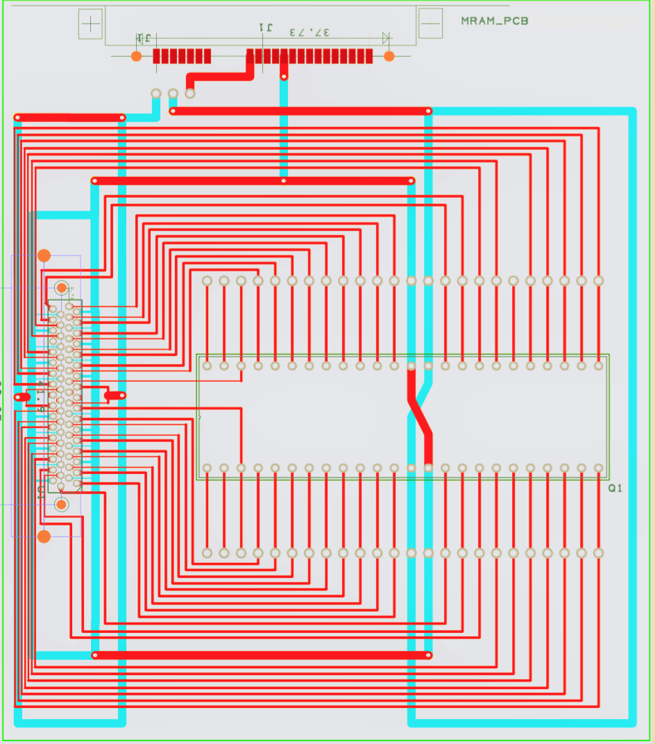
MRAM
TLC NAND Flash